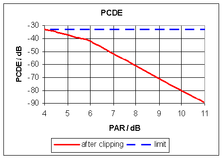
ARTICLE JUNE 2003 SYSTEM-ON-CHIP CONCEPTS FOR UMTS MULTICARRIER BASE STATION TRANSCEIVERS Mobile phone base station technology must be reconsidered to cut costs and meet the requirements of new systems, particularly third-generation (3G) UMTS. Key to the MEDEA+ A104 SCUBA project therefore is the implementation of system-on-chip (SoC) concepts for future UMTS base station radio transceiver interfaces. Defining individual analogue and digital processing functions is influenced by the characteristics of the technologies ? silicon-germanium (SiGe), CMOS and so on ? selected to realise a specific function. Transmitter and receiver up-/down-conversion analogue circuit and baseband processing demonstrators have already been developed. Work is continuing on these circuits as well as on appropriate algorithms for signal processing. Unlike current base stations, UMTS requires multi-carrier front ends and highly efficient power amplifiers. Transmitted signal processing involves further treatment of the pre-processed baseband signal ? including pulse shaping and up-conversion from baseband to radio frequency (RF). The transmitted signal is fed through a non-linear power amplifier to the aerial, requiring intelligent linearisation of the power amplification chain to achieve maximum signal quality and power efficiency. Received signal processing involves down-conversion of the radio frequency signal, which transports several RF carriers ? key to wideband code-division multiple-access (WCDMA), for example. Future multicarrier base station transceivers for mobile multimedia communications will also have to process signals with a high bandwidth (e.g. 60 MHz for a complete UMTS band) and a high ratio of peak power to average power. This results from the modulation and multiple access methods used in WCDMA and other standardised radio interfaces, and from the fact that the signals are sums of several independent carriers. The requirements for amplitude resolution will grow when even higher modulation formats are used in UMTS ? such as for the high-speed downlink packet access (HSDPA) data service. Developing chips and algorithms To meet the tough requirements of modern wireless standards at competitive cost, analogue and digital hardware is required, advantageously realised as application-specific integrated circuits (ASICs), as well as algorithms for conditioning the signals and compensating for distortions in the analogue hardware. As a result of using these techniques, transceiver modules can be reduced in size and cost, and power consumption can be cut for the same output level to enhance power efficiency. One of the main challenges in the transmitter is to operate the power amplifier in such a way that adjacent channel interference due to non-linear distortions is below a given threshold and the power efficiency is maximised. The solution is the use of advanced soft-clipping algorithms to reduce the peak-to-average ratio of the signal without distortion, with adaptive pre-distortion algorithms in the digital baseband for linearising the overall characteristic of the transmitter. Since the adaptive pre-distortion algorithm needs a feedback signal from the power amplifier output, this signal must be synchronised with the transmitted signal. This requires an additional adaptive time-delay compensation algorithm, which provides high-precision compensation for the varying time delay in the analogue signal path. Since the transmitted signal is non-linearly pre-distorted, its bandwidth is at least three times the bandwidth of the desired multicarrier signal, which means that analogue components in the transmitting path have to support this bandwidth. The acceptable linear distortions in the transmitting path are limited by the required precision of the pre-distortion to achieve a sufficiently small adjacent channel interference. Demonstrating a multicarrier transmitter One of the objectives of the SCUBA project is to build a demonstrator for a linearised multicarrier transmitter using four-carrier WCDMA signals with analogue ASICs in the transmitting and feedback paths, and prototype realisations of the linearisation algorithms in field programmable gate arrays (FPGAs). With the current demonstrator, it has been shown that the peak-to-average ratio of the digitally generated multicarrier signals can be reduced in realtime operation, being 4.5 to 5.5 dB, depending on the signal type, while meeting the 3GPP standard requirements for signal quality for peak code domain error (PCDE) ? see Figure 1.
Figure 1:Peak code domain error (PCDE) of a clipped four-carrier WCDMA signal as a function of the peak-to-average ratio (PAR) after clipping. The limit required by the 3GPP standard is -33 dB, which is met for PARs up to 4.5 dB.
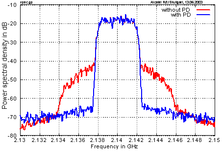
Furthermore, joint operation of the adaptive time-delay compensation and pre-distortion algorithms could be demonstrated for single and multicarrier signals. Power efficiencies between 14 and 15% for a complete transmitter module could be achieved with a power amplifier chain that is not yet optimised. With further improvements, efficiencies up to 18% are expected. The adaptive pre-distortion can reduce the intermodulation products resulting from power amplifier non linearities by more than 20 dB ? see Figure 2.
Figure 2: Power amplifier output signal at 40 W output power with and without pre-distortion. Adjacent channel power is reduced to meet requirements for adjacent channel interference.
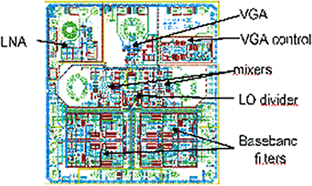
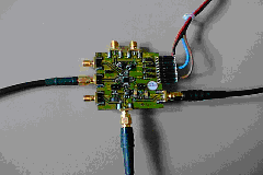
Minimising mutual RF interference It is particularly important to cut the number of analogue RF components for the receiver and to minimise the mutual interference of the individual carriers of the multicarrier signal. The reduction in analogue components can be obtained by using a direct down-conversion receiver with only one analogue down-converter stage. This receiver is based on SiGe hetero-junction bipolar technology (HBT). The layout of the chip as well as the evaluation board is shown in Figures 3a and 3b.
Figures 3a-b: Layout of chip and evaluation board for the direct down-conversion receiver (chip size: 2.55 x 2.55 mm2).
Since the required high image rejection ratios cannot be achieved with an analogue down-converter, an additional compensation algorithm is required in the digital baseband to compensate for gain and phase imbalances in the analogue section. A concept for a compensated direct down-conversion receiver has therefore been developed in SCUBA. Theoretical studies and simulations of the analogue and digital sections show that the required image rejection ratio of more than 60 dB can be achieved. First samples of analogue ASICs for down-conversion and baseband filtering are available. A prototype implementation of the digital error compensation algorithm is currently being tested. | |||