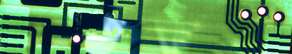
ARTICLE MAY 2001 Faster, more reliable test platforms for wafers and packaged devices An essential, if unglamorous, area of semiconductor technology is the testing required to ensure that wafer fabrication is efficient and that each device meets required specifications. The aim of MEDEA project T615 was to provide innovative solutions for this area and so improve the competitiveness of the European microelectronics industry. Challenges included the demand for faster, more reliable and cost-effective test techniques as throughput and complexity in manufacturing increase and die sizes shrink. The importance of testing during both the wafer fabrication process and when devices are finished is driven by the need for efficiency during manufacturing and, finally, for reliable, functional packaged devices. MEDEA project T615 set out to develop advanced test platforms that would position Europe ahead of competitors in the USA and Japan. The project involved a number of leading European semiconductor and test equipment manufacturers, including ELMOS, Altis Semiconductor (formerly IBM-France), Multitest, Schlumberger ATE, STMicroelectronics, Atmel Wireless & Microcontrollers (formerly TEMIC Semiconductors) and UPSYS. There were two clear development goals to the project. The first was to develop a 'vertical probe' wafer contacting system, for which the world market is forecast to grow from nearly 116 million Euros in 2000 to 290 million Euros in 2005. The second was an integrated test cell for testing packaged devices, with a world market of over 200 units, worth 99 million Euros. The theory of identifying faulty dies and high failure rate processes on the wafer, before expensive packaging takes place, is the same, but the process of testing wafers differs from process to process and application to application. For example 0.18 micron prototype processes may have a very high failure rate initially, but whilst smartcard chips can be tested very quickly and in great quantities, microprocessors have to be tested individually and can take several minutes each to complete a test cycle. Problems with conventional test platforms, which usually involve the use of cantilevered pins or probes onto the wafer, involve reliability and speed, as well as wear on the pins, which can mean frequent maintenance stops, as well as reduction in accuracy. During project T615 UPSYS developed a vertical probe system which gives more reliable contact with less wear, increasing the number of dies that can be tested in parallel, which is especially important for high volume devices, such as microcontrollers and components for mobile phones. The 'probe card' system uses micro-machined silicon probes to provide the 50 to 80 micron spacing required for next generation of wafers. Project partner Altis Semiconductors already has a system in operation called Cobra, which uses wire probes with a spacing a 100 to 150 microns. Not all products need to be tested at the wafer stage. Testing still needs to be carried out as dies can be damaged as they are being packaged and mechanical integrity must be checked. A test cell was developed during the project that allowed both electrical and mechanical tests to be handled at the same time. Previously unavailable, this modular system is also designed to work with a range of existing test equipment. The main feature of the test cell is the ease by which it can be calibrated. Using a 'golden' device, which sets the standard for all of the ICs being tested, the cell can re-circulated it whenever required and has the test software programmed into its memory. This avoids the traditionally inefficient method of having to disconnect the process and run a specially downloaded test programme. | |||